AWS Quantum Technologies Blog
Design quantum integrated circuits with open-source software DeviceLayout.jl from AWS
Today, we are introducing DeviceLayout.jl, a software package for computer-aided design (CAD) of quantum integrated circuits. At the AWS Center for Quantum Computing (CQC), we use DeviceLayout.jl to design superconducting quantum devices on our path to building a fault-tolerant quantum computer—devices we’ve used for experiments like “Hardware-efficient error correction using concatenated bosonic qubits” (our “Ocelot” chip). We developed it to help designers iterate on device layouts quickly and at scale, with particular attention to scalability in support of both larger quantum processors and a larger, collaborative team.
In this post, we highlight an example layout of a 17-qubit processor using a schematic-driven workflow in a modular, reproducible project. We then show how DeviceLayout.jl works together with Palace, an open-source tool for electromagnetic finite-element analysis also developed at the CQC.
We are releasing DeviceLayout.jl on GitHub as an open-source project, where it joins Palace as part of an open-source toolchain for electronic design automation (EDA) of quantum integrated circuits and other electromagnetic devices.
Why did we build DeviceLayout.jl?
Quantum hardware developers face challenges brought on by the combined need for exploration and scale. Quantum computing research groups often demonstrate novel technologies at the scale of a few qubits, but validating a path towards using those technologies in an error-corrected quantum processor can require experiments with tens of qubits. To help exploratory work influence the development of quantum computing hardware, we wanted to make it easy to scale novel design concepts and to incorporate novel elements into existing designs.
In particular, designers need a way to manage complexity as devices scale and teams grow. Our decisions during development have been guided by our aim to accelerate design cycles even as devices become more complex and workflows become more collaborative. With DeviceLayout.jl, chip designers can use schematic-driven layout to specify devices at a high level while independently iterating on components. They can do this entirely in code using standard software development tools for version control and reproducible environments. In part for this reproducibility, we chose to develop DeviceLayout.jl as a package for the Julia programming language, a high-performance, developer-friendly language with a rich ecosystem for technical computing, which has a best-in-class package manager and dependency resolver, Pkg.jl. In the first example below, we show how DeviceLayout.jl can be used to manage complexity with schematic-driven layout of a 17-qubit processor.
As devices reach larger component counts, it’s especially important for layout generation to integrate well into a scalable EDA workflow. We previously released Palace to enable customers to scale up 3D finite-element electromagnetic simulations on AWS, including on Graviton processors. Customers have requested a reliable way to generate device models and meshes suitable for use with Palace, and DeviceLayout.jl provides a solution. The second example below demonstrates this simulation workflow with the tuneup of a transmon qubit and readout resonator using a closed-loop optimization routine.
Quantum processor with 17 qubits
In this example, we demonstrate the layout of a 17-transmon quantum processor. As our guide, we used well-documented layouts published by the Quantum Device Lab at ETH Zurich—including those in Krinner et al., “Realizing repeated quantum error correction in a distance-three surface code”, Nature (2022) and Besedin, Kerschbaum, et al., “Realizing Lattice Surgery on Two Distance-Three Repetition Codes with Superconducting Qubits” (2025).
The schematic-driven layout workflow consists of the following steps:
- Define the component types that will appear in the device—resonators, transmons, and so on. For this example, we use predefined component types from DeviceLayout.jl’s ExamplePDK module, intended for tests and demonstrations. (A PDK is a “process design kit”, containing information about fabrication processes needed to generate layouts as well as components using that process.)
- Assemble a specification for a schematic as a graph, comprising component instances and connections between them—including special route components that define wires to be automatically routed after other components are placed.
- Calculate component placement for the schematic based on the specification by running an automated floorplanning routine.
- Check that this schematic (the specification along with component position and orientation) follows high-level design rules—for example, that all Josephson junctions have the correct orientation for the intended fabrication process.
- Make any desired changes or additions based on the results of floorplanning, like creating crossovers between intersecting wires or filling the empty areas of the ground plane with holes for flux trapping.
- Render the schematic, generating 2D geometry for each component for output in a format like GDSII.
Schematic-driven layout allows the designer to work with a high-level description of the device independent of the detailed geometry. The component definitions specify what geometry to draw and, together with the automated floorplanning routine, ensure that they line up correctly with other components. Designers can edit components without needing to manually track and correct far-reaching changes through the entire device, and they can easily reuse components in different schematics.
You can find a detailed walkthrough of each step in this example in the DeviceLayout.jl documentation, with the full code in the package repository on GitHub. Figure 1 illustrates the output of running the example script, which returns the schematic and the “artwork” containing the layout for fabrication. We visualize the schematic using a false-color drawing where each component’s footprint is drawn in a layer corresponding to that component’s role, and we save both that drawing and the artwork in a standard graphical format:
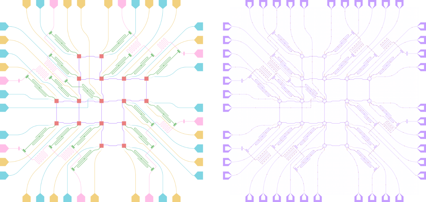
Figure 1: False-color schematic (left) and artwork (right) for the quantum processor. The false-color schematic shows the 17 transmons in red, the couplers between them in purple, and the readout resonators and filters in green. The XY control, Z control, and readout lines are blue, gold, and pink, respectively. The artwork shows the actual geometry that would be used for fabrication, with the areas where metal will be removed in purple, as well as small features for other process steps like air bridges and Josephson junctions.
Because the code that generates this layout is a Julia project, the Julia package manager generates a manifest with exact versions of all of the project’s dependencies (including transitive dependencies), which it can then instantiate anywhere with a connection to the package registry. Users can also leverage the package manager with their own versioned PDK containing their components and process technology information. This allows design projects to be portable, reproducible, and collaborative.
Electromagnetic simulation with Palace
We can also use a schematic to create a 3D model and a simulation configuration, addressing the challenge Palace users face of preparing their own finite element meshes for use with the solver. For this example, we use the transmon and readout resonator shown in the Palace release announcement. This example is much simpler than the processor above, but we follow the same steps to create a schematic.
Instead of rendering the “native” DeviceLayout.jl geometry to a 2D representation using polygons, we render a full 3D model with a backend provided by the Open CASCADE Technology geometry library. The renderer first draws 2D shapes on the appropriate plane, including exact representations of curvilinear elements like circular arcs and splines. It then performs operations like differences and extrusions to create the 3D geometry, including elements like air bridges, according to instructions provided by the PDK.
Once the 3D geometry is created, we generate a mesh using the Julia interface to Gmsh. Because our 3D renderer supports curves, we can produce a mesh that follows the bends in our coplanar-waveguide resonator using our desired settings (for example with high-order elements) without relying on a prior discretization. The mesh sizing is also informed by the native geometry description, including hints added by component developers to shapes where resolving the electromagnetic fields is expected to take a finer mesh. Figure 2 illustrates the model and mesh output by the example script.
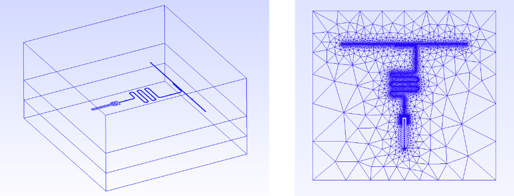
Figure 2: 3D model (left) and mesh of the metal surfaces (right) in the transmon-resonator model, viewed in the Gmsh GUI.
To configure a simulation with Palace, we populate a configuration template by identifying the volumes and surfaces in the mesh to assign to each material and boundary condition. Palace identifies entities in the mesh by unique integer labels called “attributes”. Meanwhile, by construction, our 3D model contains named “physical groups” organizing geometric entities by physical meaning—substrate, vacuum, metal, ports, Josephson junctions—and maps each group to an attribute. We use this mapping to configure a simulation according to the physical intent behind the model, without having to worry about how the underlying geometry or attribute numbering might change.
With our mesh and configuration, we’re now prepared to run Palace, which computes the eigenfrequencies of the transmon and resonator modes. After it finishes, we parse the results in Julia. Moreover, once this is set up, we can wrap CAD, meshing, and eigenfrequency analysis into an optimization routine, for example using one of many classical or modern methods available through the Julia ecosystem. For this demonstration, we use PRIMA to tune our modes to within 1% of our target frequencies:
julia> SingleTransmon.run_optimization("/path/to/palace", 8)
Number of Palace runs: 9
Initial parameters:
    Transmon capacitor_length = 620.0μm
    Resonator total_length = 5000.0μm
Initial frequencies: [4.14, 5.591] GHz
Final parameters:
    Transmon capacitor_length = 1217.678 μm
    Resonator total_length = 7243.955 μm
Final frequencies: [3.005, 3.982] GHz
This takes about 40 minutes with Palace running with 8 processes on a single m6i.4xlarge instance. While we might want to find a more compute-efficient way to tune up a real device, this serves as a demonstration of a robust closed loop incorporating everything from schematic specification to 3D finite element analysis. This pipeline, which uses only open-source software, creates many powerful options for electronic design automation.
The full code for this example is available on GitHub, with a detailed walkthrough in the DeviceLayout.jl docs.
Full-chip simulation
We’re not limited to modeling, meshing, and simulating schematics with just a few components. We can take our 17-qubit device from above, render a 3D model, mesh it, and generate a configuration in the same way. Simulating the whole chip, we find the eigenmodes of our resonators and transmons, their dissipation into ports on each coplanar-waveguide launcher on the perimeter of the chip, and the energy participation ratio of junctions in each mode. Figure 3 illustrates a 3D model and mesh of the device, and Figure 4 illustrates the results of eigenfrequency simulation with Palace.
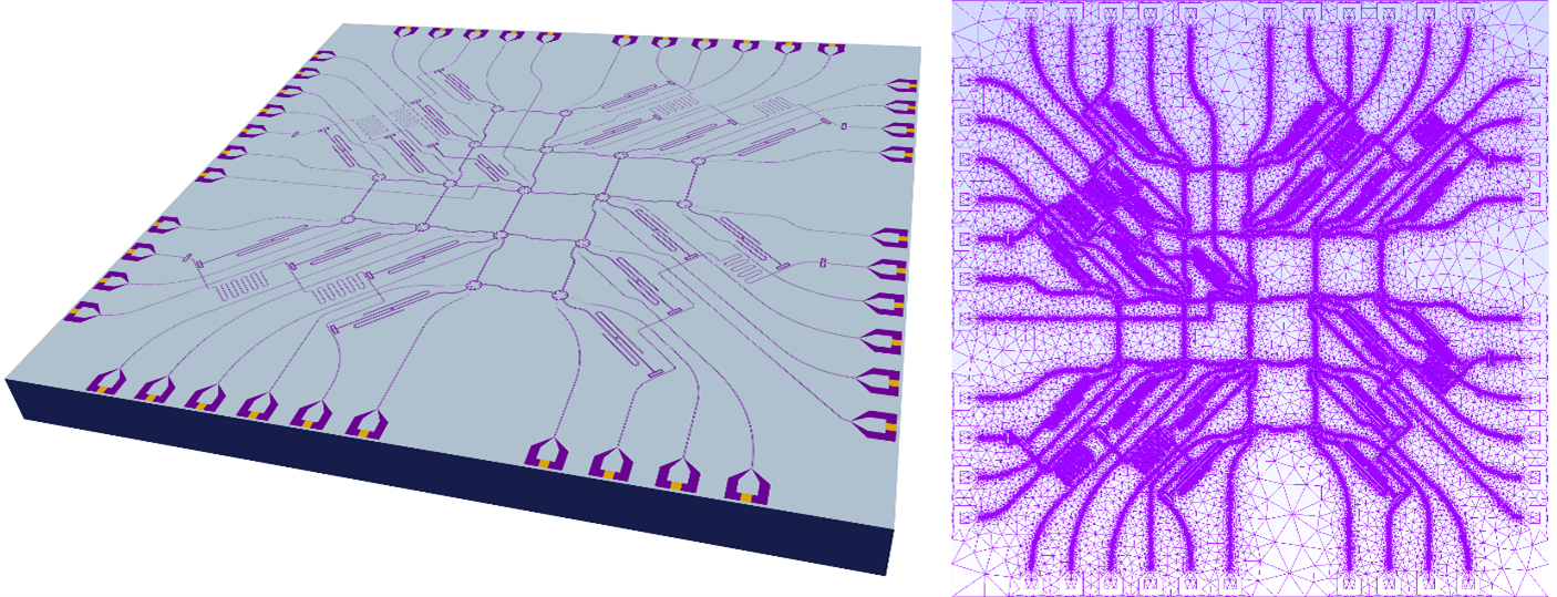
Figure 3. Left: 3D chip model based on the layout from Figure 1, including lumped ports (gold), visualized using ParaView. Right: Mesh of metal surfaces, viewed in the Gmsh GUI.
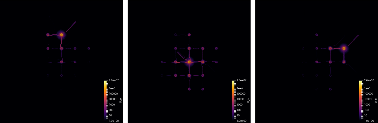
Figure 4: Electric field energy density (log scale, arbitrary units) on a plane near the chip surface for three different transmon modes, visualized using ParaView. All transmon modes are near the same frequency and show some hybridization with one another depending on proximity. For a given transmon mode, energy density near neighboring transmons is smaller by orders of magnitude.
You don’t always need to simulate an entire chip in full detail, but this example demonstrates the potential of the DeviceLayout.jl/Palace toolchain for studying processor-scale questions.
Get started
This blog post introduced DeviceLayout.jl, a newly released, open-source layout package for quantum integrated circuits. We also showed examples using this software for layout of a 17-qubit processor and for preparing models for electromagnetic simulations. DeviceLayout.jl is licensed under the MIT license and is free to use. You can learn how to get started with the quick-start guide in the project documentation, which also includes full walkthroughs of the examples above. You can also check out the DeviceLayout.jl GitHub repository, where you can file issues and learn about contributing to the project.